


Communication Manager Maintenance-Object Repair Procedures
2000 Maintenance Procedures for Avaya Communication Manager 3.0, Media Gateways and Servers
SNC-BD (Switch Node Clock Circuit Pack)
S8700 MC
The Switch Node Clock (SNC) TN572 circuit pack is part of the Center Stage Switch (CSS)
configuration. It resides in a switch node carrier that alone or with other switch nodes make up a
CSS. In a high-reliability system (duplicated server and control network, unduplicated PNC),
each SNC is duplicated such that there are two SNCs in each switch node carrier. In a
critical-reliability system (duplicated server, control network, and PNC), each switch node is fully
duplicated, and there is one SNC in each switch node carrier. SNCs are placed in slots 10 and
12 of the switch node carrier.
The active SNC communicates with each circuit pack in the switch node carrier over the serial
channel bus on the backplane. In addition, the active SNC provides timing to the circuit packs in
the switch node carrier via the clock buses. The active SNC uses Timing Priority Number (TPN)
links with each Switch Node Interface (SNI) and the other SNC to receive and distribute TPNs.
TPNs are used for setting up the correct timing distribution for the switch node carrier. The
active SNC receives timing for the switch node carrier from each SNI circuit pack in the carrier
and chooses the SNI with the best timing reference for the switch node carrier timing signal the
SNC puts out on the clock buses. The timing reference for each SNI is derived from the fiber
signal to each SNI. The active SNC chooses the SNI to receive timing from by choosing the SNI
with the lowest numbered TPN which means that the SNI is closest to the system timing source.
The active SNC also verifies that the SNI reference signal is good before using that SNI as the
timing reference for the switch node carrier. The active SNC then supplies this timing over the
clock buses on the backplane to every SNI and SNC circuit pack in the carrier. For more
information about timing synchronization (including how the SNC fits into the overall
synchronization configuration), see SYNC (Port-Network Synchronization)
on page 2143.
The SNC circuit packs are associated with three MOs:
● The SNC-BD (Switch Node Clock Circuit Pack) on page 2000 MO covers general SNC
board errors and errors with the serial communication channel between the active and
standby SNCs.
● The SNC-LINK (Switch Node Clock Link) on page 2039 MO covers errors between the
active SNC and SNIs over the serial channel (Aux Data is 1). Also, the SNC-LINK MO
covers TPN Link errors between the active SNC and SNIs (Aux Data is 2).
● The SNC-REF (Switch Node Clock Reference) on page 2043 MO covers errors the active
SNC detects with SNI reference signals.
SNC circuit packs are part of port-network connectivity (PNC). For background information
about PNC, refer to the Maintenance Architecture and Hardware Configurations chapters.
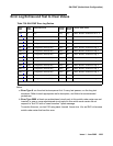
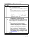
MO Name Alarm Level Initial SAT Command to Run Full Name of MO
SNC-BD MAJ test board location s SNC Circuit Pack
SNC-BD MIN test board location s SNC Circuit Pack