


APPENDIX
App. - 27
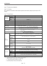
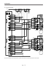
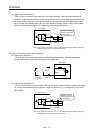
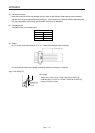
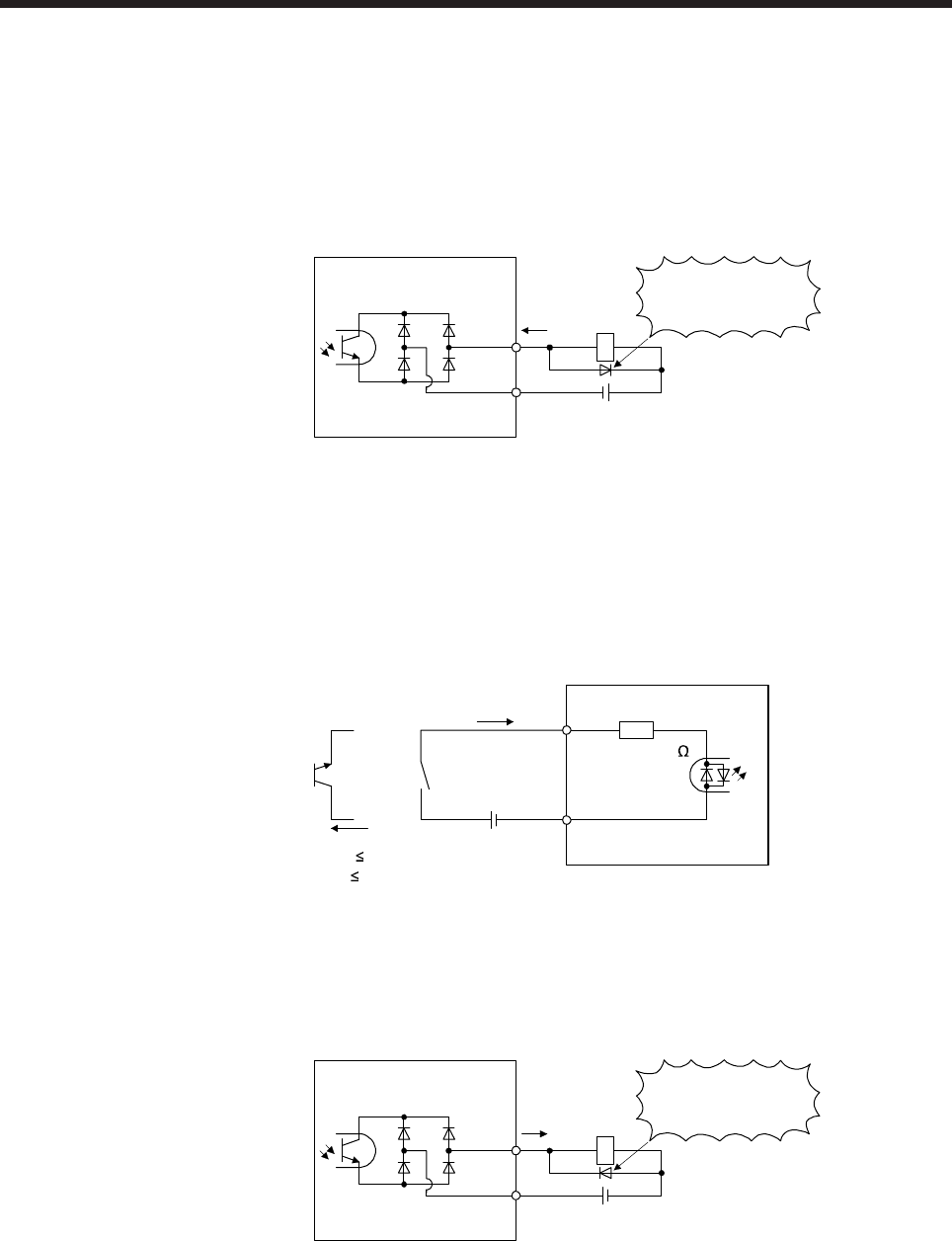
(b) Digital output interface DO-1
This is a circuit of collector output terminal of the output transistor. When the output transistor is
turned on, collector terminal current will be applied for the output. A lamp, relay or photocoupler can
be driven. Install a diode (D) for an inductive load, or install an inrush current suppressing resistor
(R) for a lamp load. (Rated current: 40 mA or less, maximum current: 50 mA or less, inrush current:
100 mA or less) A maximum of 2.6 V voltage drop occurs in the MR-J3-D05.
If polarity of diode is
reversed, MR-J3-D05
will malfunction.
(Note) 24 V DC ± 10%
200 mA
MR-J3-D05
SDO2B+,
etc.
SDO2B-,
etc.
Load
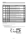
Note. If the voltage drop (maximum of 2.6 V) interferes with the relay operation, apply high
voltage (maximum of 26.4 V) from external source.
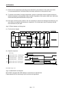
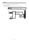
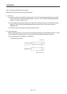
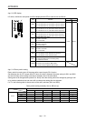
(2) Source I/O interfaces (CN9, CN10 connector)
(a) Digital input interface DI-1
This is an input circuit whose photocoupler anode side is input terminal. Transmit signals from
source (open-collector) type transistor output, relay switch, etc.
V
CES
1.0 V
I
CEO
100 µA
Approximately 5 mA
24 V DC ± 10%
200 mA
Switch
SRESA-,
etc.
MR-J3-D05
SRESA+,
etc.
Approx. 5.4 k
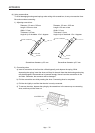
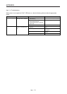
(b) Digital output interface DO-1
This is a circuit of emitter output terminal of the output transistor. When the output transistor is turned
on, current will be applied from the output to a load. A maximum of 2.6 V voltage drop occurs in the
MR-J3-D05.
MR-J3-D05
If polarity of diode is
reversed, MR-J3-D05
will malfunction.
(Note) 24 V DC ± 10%
200 mA
Load
SDO2B+,
etc.
SDO2B-,
etc.
Note. If the voltage drop (maximum of 2.6 V) interferes with the relay operation, apply high
voltage (maximum of 26.4 V) from external source.