


3 - 35 3 - 35
MELSEC-Q
3 SPECIFICATIONS
(10) Each Node Communication Error Status (addresses 1C0
H
to
1C3
H
/448 to 451)
These addresses store whether an I/O communication error has occurred or not
for each slave node set to the "parameters for the master function" when I/O
Communicating (X01) is ON.
Note that the error is not detected for the node where "Down Node Detection
Disable Status (addresses 01CC
H
to 01CF
H
/460 to 463)" has been set.
• When the corresponding bit is ON : Communication error exists.
• When the corresponding bit is OFF: Communication error does not exist.
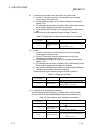
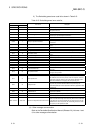
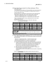
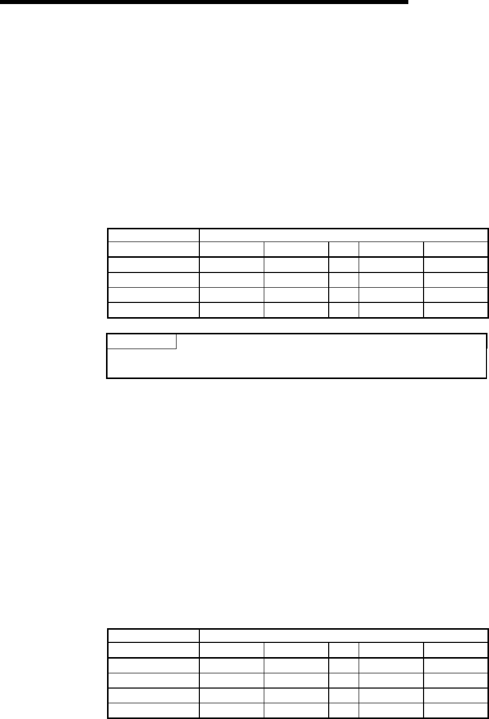
Table 3.19 indicates the buffer memory addresses and the node number
corresponding to each bit.
Table 3.19 Corresponding Node Number of Each Bit in Each Node
Communication Error Status
Buffer memory address Corresponding node number of each bit
(hexadecimal) Bit 15 Bit 14
…
Bit 1 Bit 0
01C0
H
Node 15 Node 14
…
Node 1 Node 0
01C1
H
Node 31 Node 30
…
Node 17 Node 16
01C2
H
Node 47 Node 46
…
Node 33 Node 32
01C3
H
Node 63 Node 62
…
Node 49 Node 48
POINT
When any of the bits in the "Each Node Communication Error Status" area turns
ON, Slave Down Signal (X04) turns ON.
(11) Each Node Obstacle Status (addresses 01C4
H
to 01C7
H
/452 to 455)
These addresses store whether or not a communication problem had occurred in
each slave node.
• When the corresponding bit is ON: Problem information exists.
• When the corresponding bit is OFF: No error information exists.
Use the following procedure to turn OFF the corresponding bit.
(a) Using the message communication area of the buffer memory, execute the
readout of the communication error information of the corresponding node.
(For information on the readout of communication error information, see
Section 3.4.2, (1) message communication command, (2) message
communication result, and (3) message communication data.)
(b) When the readout of communication error information is executed, the
corresponding bit is automatically turned OFF.
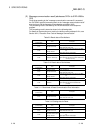
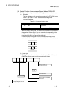
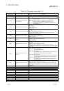
Table 3.20 lists the buffer memory address and node number corresponding
to each bit.
Table 3.20 Corresponding node number of each bit when each node is in
obstacle status
Buffer memory address Corresponding node number of each bit
(hexadecimal) Bit 15 Bit 14
…
Bit 1 Bit 0
01C4
H
Node 15 Node 14
…
Node 1 Node 0
01C5
H
Node 31 Node 30
…
Node 17 Node 16
01C6
H
Node 47 Node 46
…
Node 33 Node 32
01C7
H
Node 63 Node 62
…
Node 49 Node 48