


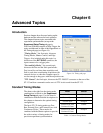
Chapter 5 Operation 47
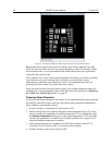
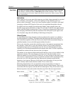
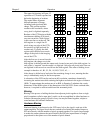
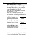
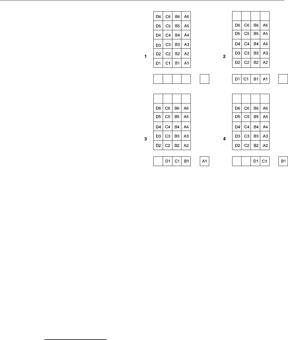
The upper left drawing in Figure 12
represents a CCD after exposure but
before the beginning of readout.
The capital letters represent
different amounts of charge,
including both signal and dark
charge. This section explains
readout at full resolution, where
every pixel is digitized separately.
Readout of the CCD begins with the
simultaneous shifting of all pixels
one row toward the “shift register,”
in this case the row at the top. The
shift register is a single line of
pixels along one edge of the CCD,
not sensitive to light and used for
readout only. Typically the shift
register pixels hold twice as much
charge as the pixels in the imaging
area of the CCD.
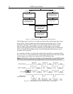
After the first row is moved into the
shift register, the charge now in the
Figure 12. Full Frame at Full Resolution
shift register is shifted toward the output node, located at one end of the shift register. As
each value is “emptied” into the output it is digitized. Only after all pixels in the first row
are digitized is the second row moved into the shift register. The order of shifting in our
example is therefore A1, B1, C1, D1, A2, B2, C2, D2, A3, ….
After charge is shifted out of each pixel the remaining charge is zero, meaning that the
array is immediately ready for the next exposure.
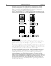
A subsection of the CCD can be read out at full resolution, sometimes dramatically
increasing the readout rate while retaining the highest resolution in the region of interest
(ROI). To approximate the readout rate of an ROI, in Equation 2 substitute the x and y
dimensions of the ROI in place of the dimensions of the full CCD. Some overhead time,
however, is required to read out and discard the unwanted pixels.
Binning
Binning is the process of adding the data from adjacent pixels together to form a single
pixel (sometimes called a super pixel), and it can be accomplished in either hardware or
software. Rectangular groups of pixels of any size may be binned together, subject to
some hardware and software limitations.
Hardware Binning
Hardware binning is performed on the CCD array before the signal is read out of the
output amplifier. For signal levels that are readout noise limited this method improves
S/N ratio linearly with the number of pixels grouped together. For signals large enough
to render the camera photon shot noise limited, the S/N ratio improvement is roughly
proportional to the square root of the number of pixels binned.