


FORM 50.40-OM2
71YORK INTERNATIONAL
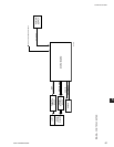
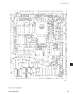
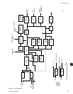
COM 1 is connected directly to the Micro. COM
2 through 5 are connected directly to the UART
(Universal Asynchronous Receive Transmit). The
UART converts the parallel data to serial form for
transmission to the peripheral device and converts the
incoming serial data to parallel form for use by the
Micro. It also generates and processes control signals
for the Modem communications (DTR, CTS, DSR,
RTS). Under Program control, the Micro instructs the
UART of the desired data transmission Baud rate. A
crystal oscillator provides the frequency reference.
Each port is equipped with two LED’S; a red one
indicates when data is being transmitted to the remote
device and a green one indicates when data is being
received from the remote device. The RS-232 output
voltages are industry standard +3 to +15VDC, with
+9VDC typical. The RS-485 output voltages are
industry standard +1.5 to +5VDC, with +2.5VDC
typical. A loopback diagnostic test can be performed
on each serial port. This test permits verication of
the data transmitted from the serial port. Refer to the
“Serial Inputs / Outputs Tests” description in this book
for details of these tests. The graphic screens that are
displayed on the Liquid Crystal Display are created
from preformed graphics and messages that are stored
in the Program (FLASH Memory Card), and real-time
system operating parameters, such as temperatures.
The graphics, message and number data are in the form
of digital words. The Display Controller converts this
data into display drive signals and sends them to the
Display from Microboard J5. The Display has 307,200
pixels arranged in a 640 columns x 480 rows matrix
conguration. Each pixel consists of 3 windows; red,
green and blue, through which a variable amount of
light from the Display backlight is permitted to pass
through the front of the display. Imbedded in each
window of the pixel is a transistor, the conduction of
which determines the amount of light that will pass.
The drive signal determines the amount of conduction
of the transistor and therefore the amount of light
passed through the window. The overall pixel color
becomes a result of the gradient of red, green and blue
light allowed to pass. The drive signal for each pixel is
an 18 bit binary word; 6 for each of the 3 colors, red,
green and blue. The greater the binary value, the greater
the amount of light permitted to pass. The pixels are
driven sequentially from left to right, beginning with
the top row. To coordinate the drive signals and assure
the pixels in each row are driven sequentially from
left to right and the columns are driven from top to
bottom, each drive signal contains a horizontal and
vertical sync signal.
The Display DRAM is a memory device that supports
the operation of the display controller. This device
could be either of two types; FPM (fast page mode) or
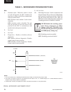
EDO (extended data out) type. Program Jumper JP6
must be positioned according to the type of DRAM
device installed in the Microboard; JP6 in - EDO,
out - FPM. Refer to Table 2, “Program Jumpers”.
Depending upon the requirement, there could be one
or two DRAM devices installed in the Microboard.
If the design requires only one DRAM, it is installed
in socket U27. If an additional one is required, it is
installed in socket U25.
During the power-up sequence, the program in the
BIOS EPROM reads Program Jumper JP6 to determine
the type of Display DRAM installed (as explained
above). It also reads wire jumpers PID0 through PID3
(via Microboard J5) on the Display Interface Board
to determine the manufacturer of the display (refer to
description of Display Interface Board). Each display
manufacturer requires a slightly different control.
The program in the BIOS EPROM then congures
the Display Controller for operation with the actual
display that is present.
Different Display manufacturers can require different
supply and control voltages for their displays and
backlights. Program Jumpers JP 2 through 4 and 5
through 8 must be congured to provide the required
supply and control voltages to the display and backlight
control. Table 2 lists the required Program Jumper
conguration for the Display. Also, a label attached to
the Display mounting plate lists the required Program
Jumper conguration for that particular Display.
The power supply voltage that operates the Display
is provided by the Microboard J5. The position of
Program Jumper JP2 determines whether this supply
voltage is +5VDC or +3.3VDC. The Display requires a
specic power-up and power-off sequencing to prevent
damage. During power-up, the supply voltage must
be applied to the Display before the drive signals are
applied. Similarly, during power-off sequencing, the
display drive signals must be removed prior to removing
the supply voltage. The Display Controller applies the
supply voltage and data drive signals to the Display in
the proper sequence. The Display Controller controls
the Display Backlight by applying control signals
(from Microboard J6) to the Backlight Inverter Board.
The Backlight Inverter Board converts low voltage
DC (+12VDC or +5VDC, depending on position of
5