


YORK INTERNATIONAL70
The BRAM (battery backed random access memory) is
a memory device that contains a battery that preserves
the data during power failures. It is a replaceable part.
Refer to the YORK Renewal Parts List. It is located
in socket location U52. The Micro stores the setpoints
programmed by the Operator or Service Technician,
History Data and other data that requires preservation,
in this device. Also, the day of week, time of day and
calendar date time-keeping are done here.
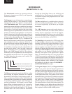
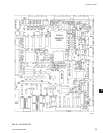
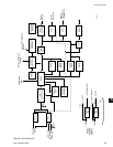
The keypad is a matrix of conductors arranged in rows
and columns (ref. Fig. 45 & 46). There are 4 rows
and 8 columns. When a key is pressed, the conductors
are pressed together at that point, creating continuity
between that row conductor and the column conductor.
The Keypad is read by applying a logic low to a row
while leaving +5VDC pullup on all the other rows. The
Micro then reads the 8 columns. If any column has a
logic low on it, the key corresponding to that coordinate
(row, column) is being pressed. The Micro reads the
entire Keypad by repeating this routine beginning
with row 1 and ending with row 4. The entire Keypad
is read every Program cycle. The Micro selects the
MUX inputs (Microboard J7, J8, J9) for input to the
A/D Converter by writing sequential addresses to the
FPGA. The FPGA holds each address until a new one
is received from the Micro. As each address is applied
to the MUX, the input corresponding to that address
is passed through the MUX to the A/D Converter.
The A/D Converter will convert the analog value to a
digital word when the Micro writes a “start conversion”
pulse to the FPGA. The FPGA passes this to the A/D
Converter. The Micro allows access to the PC-104
port (Microboard J16, J17) by writing an enable
pulse to the FPGA. The FPGA applies this to the data
transceiver, allowing data to be output to or input from
the PC-104 Port.
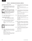
To provide flexibility for future Analog Inputs (to
Microboard J7), 2 analog inputs can be congured for either
0-10VDC or 4-20mA, Transducer or Thermistor inputs
using Program Jumpers JP21 and JP22. The position of the
jumper determines which type of input can be connected.
Refer to Fig. 36 and Table 2, “Program Jumpers”.
These inputs are for future YORK
Factory expansion use only. They
are not general application spare
inputs that will support arbitrarily
installed devices. Devices CANNOT
be connected to these inputs until
the program has been modified to
read and process the input. Unless
YORK documentation shows a device
connected to the input with a dened
function, the input cannot be used.
The Microboard receives 2 supply voltages (Microboard
J1) from the Power Supply; +12VDC, +5VDC and
Ground. The +12VDC and +5VDC are input to Voltage
Regulators to derive other regulated voltages. The
+5VDC is input to a +3.3VDC regulator. The output is
a 3.3VDC regulated voltage. The +12VDC is input to
a 5VDC regulator. The output of this regulator powers
only the Analog circuits. This includes the MUX, A/D
converter, and Thermistors. As depicted on Fig. 33,
these voltages can be monitored at Test Posts TP1
through TP6.
The Microboard is equipped with 5 Serial Data Ports
(ref. Fig. 35). Connector J2 is shared with both COM
1 and COM 4B. Each Port is dedicated for a specic
function as follows:
a. COM 1 (J2) - RS-232. Printer.
b. COM 2 (J13) - RS-232. Not Used.
c. COM 3 (J12) - RS-485. Chiller panel communica-
tions .
d. COM 4 (4A-J11), (4B-J2) - This port is actually two
ports. However, they cannot be used simultaneously;
only one of these ports can be connected to a device
at a time. The position of Microboard Program
Jumper J27 determines which port can be used
(refer to Table 2). COM 4A (J11) is an RS-485
port that is used for Multi-Unit Communications.
COM 4B (J2) is an RS-232 port that is used for
MicroGateway.
e. COM 5 (J15) – Not Used.
Service