110 Xilinx Development System
Xilinx System Generator v2.1 Reference Guide
between 16 to 4096, inclusive for the other FPGA families. The word width must be
between 1 and 1024, inclusive.
The Core datasheet for the Single Port Block Memory may be found locally at:
%XILINX%\coregen\ip\xilinx\eip1\com\xilinx\ip\blkmemsp_v3_2\do
c\sp_block_mem.pdf
The Core datasheet for the Distributed Memory may be found on your local disk at:
%XILINX%\coregen\ip\xilinx\eip1\com\xilinx\ip\c_dist_mem_v5_0\
doc\dist_mem.pdf
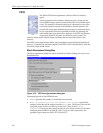
Single Port RAM
The Xilinx Single Port RAM block implements a random access
memory (RAM).
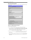
Block Interface
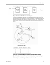
The block has one output port and three input ports for address, input data, and write
enable (WE). Values in a Single Port RAM are stored by word, and all words have the
same arithmetic type, width, and binary point position.
The block has two possible implementations, using either block or distributed
memory. Each data word is associated with exactly one address that can be any
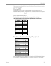
unsigned integer from 0 to
d
-1, where d denotes the RAM depth (number of words
in the RAM). An attempt to read past the end of the memory is caught as an error in
the simulation. The initial RAM contents can be specified through the block
parameters.
The write enable port must be a 1-bit unsigned integer. When the WE port is 1, the
value on the data input is written to the location indicated by the address line. The
output during a write operation depends on the choice of memory. For distributed
memory, the output port always has the value at the location specified by the address
line. For block memory, the behavior of the output port depends on the write mode
selected. When the WE is 0, the output port has the value at the location specified by
the address line.


