


315889-002 27
Control Signals
3 Control Signals
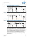
3.1 Output Enable (OUTEN) - REQUIRED
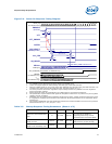
The VRM/EVRD must accept an input signal to enable its output voltage. When
disabled, the regulator’s output should go to a high impedance state and should not
sink or source current. When OUTEN is pulled low during the shutdown process, the
VRM/EVRD must not exceed the previous voltage level regardless of the VID setting
during the shutdown process. Once operating after power-up, it must respond to a
deasserted OUTEN within 500 ms. The circuitry driving OUTEN is an open-collector/
drain signal. It is EXPECTED that the pull-up resistor will be located on the baseboard
and will not be integrated into the PWM controller chip or VRM.
3.2 Voltage Identification (VID [6:0]) - REQUIRED
The VRM/EVRD must accept a 7-bit code, VID [6:0], from the processor to set the
reference Vcc operating voltage. Two VID code standards are supported within the
VRM/EVRD 11.0 specification. The first is an extended VR 10 table that is fully
compliant to the VRM/EVRD 10.2 standard, but adds an additional bit for 6.25 mV VID
resolution. (See Table 3-3) The second is a VR 11.0 standard defined in Table 3-4. The
VID_Select pin, Section 3.4, will identify which table is to be used. Designers should
note that although the VR 11.0 VID code is comprised of eight bits, VID 7 is a provision
for future Itanium-based processors. The VID 7 pin should be connected to V
SS, VO- or
GND on the VRM module’s printed circuit board. The platforms targeted by this design
guideline will only require VID [6:0].
If an “OFF” VID code is received, such as when no processor is installed, the regulator
must disable its output voltage. If this disable code appears during previously normal
operation, the regulator shall turn off its output within 500 ms. The circuitry driving
each VID [6:0] signal can be an open-collector/drain or a push-pull output type gate.
When driven by an open-collector / drain, these VID signals need to be pulled-up to the
processor’s VTT voltage. Consult the appropriate platform design guide for the
recommended pull-up resistor value. A typical value used is 510 Ohms. When driven by
a push-pull output gate, the pull-up resistors are optional. Consult the appropriate
processor EMTS for driver definition. Pull-ups to 12 V or 5 V are not supported by the
CPU package and therefore are not permitted. It is EXPECTED that the pull-up
resistors will be located on the baseboard and will not be integrated into the PWM
controller chip or VRM.
Note: 1) Other platform components may use VID inputs and may require tighter limits.
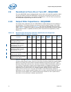
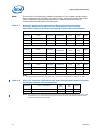
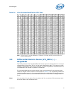
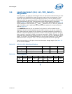
Table 3-1. OUTEN Specifications
Symbol Parameter Min Max Units
VIH Input Voltage High 0.8 3.465 V
VIL Input Voltage Low 0 0.4 V
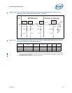
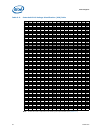
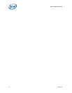
Table 3-2. VID [6:0] Specifications
Symbol Parameter Min Max Units Notes
V
IH
Input High Voltage 0.8 VTT max V 1
V
IL
Input Low Voltage 0 0.4 V 1