


315889-002 17
Output Voltage Requirements
dependent upon the selection of the bulk capacitors, ceramic capacitors, power plane
routing and the tuning of the PWM controller’s feedback network. This analysis can be
done with LGA771-V2 VTT tool impedance testing or through power delivery simulation
if the designer can extract the parasitic resistance and inductance of the power planes
on the motherboard along with good models for the decoupling capacitors.
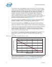
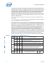
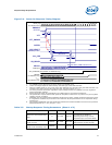
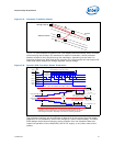
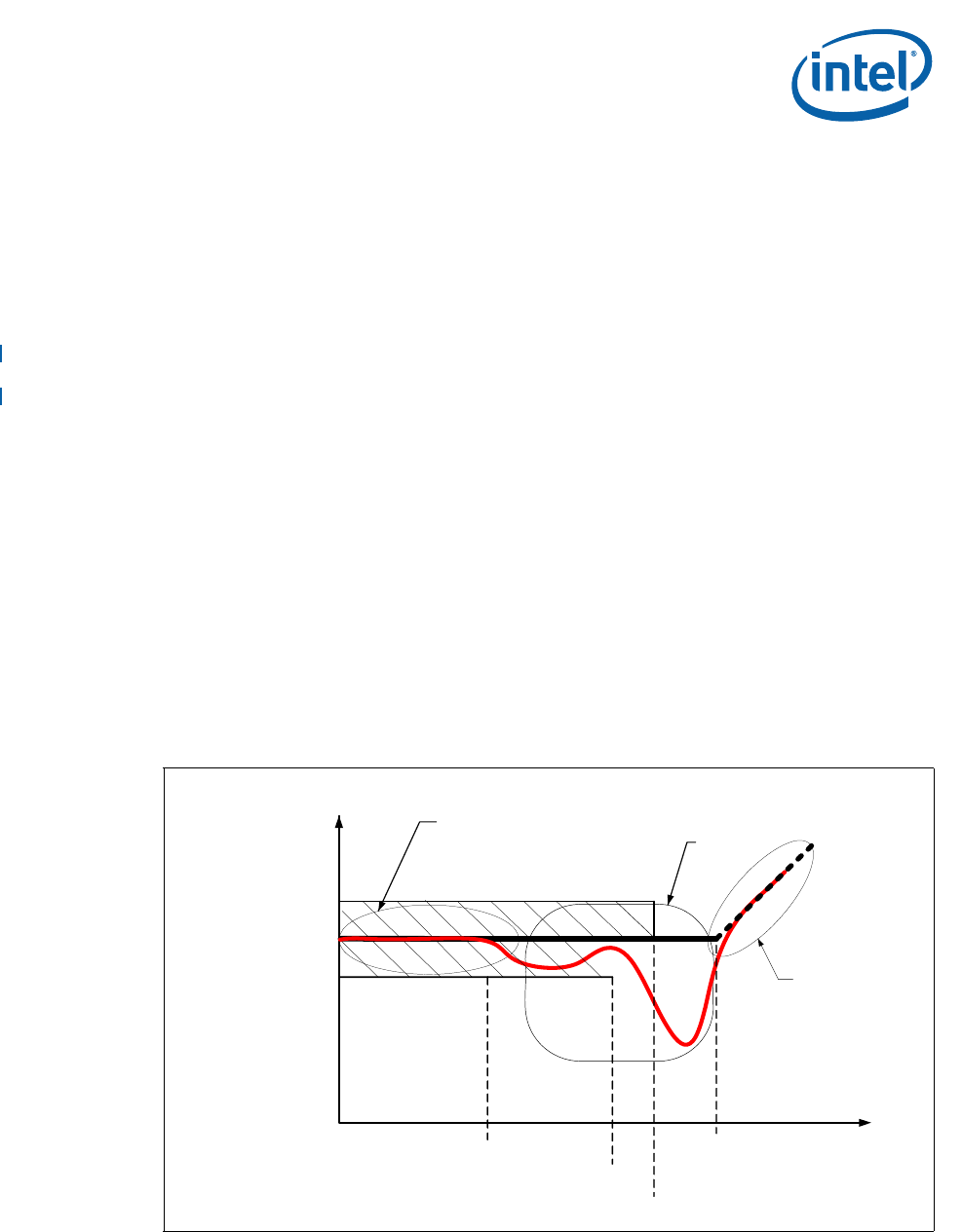
Measured power delivery impedance should be within the tolerance band shown in
Figure 2-3. The tolerance band is defined for the VTT impedance measurement only.
For load line compliance, time domain validation is required and the VR tolerance band
must be met at all times. Above 500 kHz, the minimum impedance tolerance is not
defined and is determined by the MLCC capacitors required to get the ESL low enough
to meet the load line impedance target of the F
BREAK frequency. At 700 kHz, the ZMAX
tolerance drops to the load line target impedance. Any resonance point that is above
the ZMAX line needs to be carefully evaluated with the time domain method by applying
transient loads at that frequency and looking for V
MAX or VMIN violations. Maintaining
the impedance profile up to FBREAK is important to ensure the package level decoupling
properly matches the motherboard impedance. After FBREAK, the impedance
measurement is permitted to rise at an inductive slope. The motherboard VR designer
does not need to design for frequencies over F
BREAK as the Intel Microprocessor
package decoupling takes over in the region above FBREAK.
Each of these design elements should be fully evaluated to create a cost optimized
solution, capable of satisfying the processor requirements. Experimental procedures for
measuring the Z(f) profile will be included (shortly) in the next revision of the
EVRD_VRM11_0_LL_dVID LGA771_775-V2 VTT Tester-UG.pdf Test Methodology User’s
Guide using the VTT. Additional background information regarding the theory of
operation is provided in Appendix A.
Notes:
1. Zone 1 is defined by the VR closed loop compensation bandwidth (VR BW) of the voltage regulator.
Typically 30-40 kHz for a 300 kHz voltage regulator design
2. Zones 2 & 3 are defined by the output filter capacitors and interconnect parasitic resistance and
inductance. The tolerance is relaxed over 500 kHz allowing the VR designer freedom to select output filter
capacitors. The goal is to keep Z(f) below Z
LL up to FBREAK (2 MHz) and as flat as practical, by selection of
bulk cap values, type and quantity of MLCC capacitors. The ideal impedance would be between Z
LL and
Z
LLMin, but this may not be achieved with standard decoupling capacitors.
Figure 2-3. Power Distribution Impedance vs. Frequency
Hz
Z target = Z
LL
F
break
Z
LL Min
VR BW
Zone 1
PWM Droop control
& compensation BW
500 kHz
700 kHz
Zone 2
Output Filter
Bulk & MLCC
Zone 3
Inductive effects
MLCC ESL +
Socket
Z
LL Max