


315889-002 21
Output Voltage Requirements
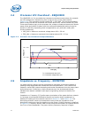
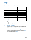
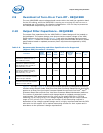
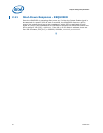
Figure 2-6 is an example of dynamic VID. The diagram assumes steady state, constant
current during the dynamic VID transition for ease of illustration; actual processor
behavior allows for any dIcc/dt during the transitions, depending on the code it is
executing at that time. Note that during dynamic VID, the processor will not output VID
codes that would disable the voltage regulator output voltage.
The processor load may not be sufficient to absorb all of the energy from the output
capacitors on the baseboard, when VIDs change to a lower output voltage. The VRM/
EVRD design should ensure that any energy transfer from the capacitors does not
impair the operation of the VRM/EVRD, the AC-DC supply, or any other parts of the
system.
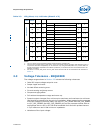
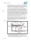
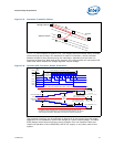
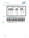
Figure 2-5. Processor Transition States
VID High Load Line
1
2
3
4
Icc-max
5
VID Low Load Line
A
B
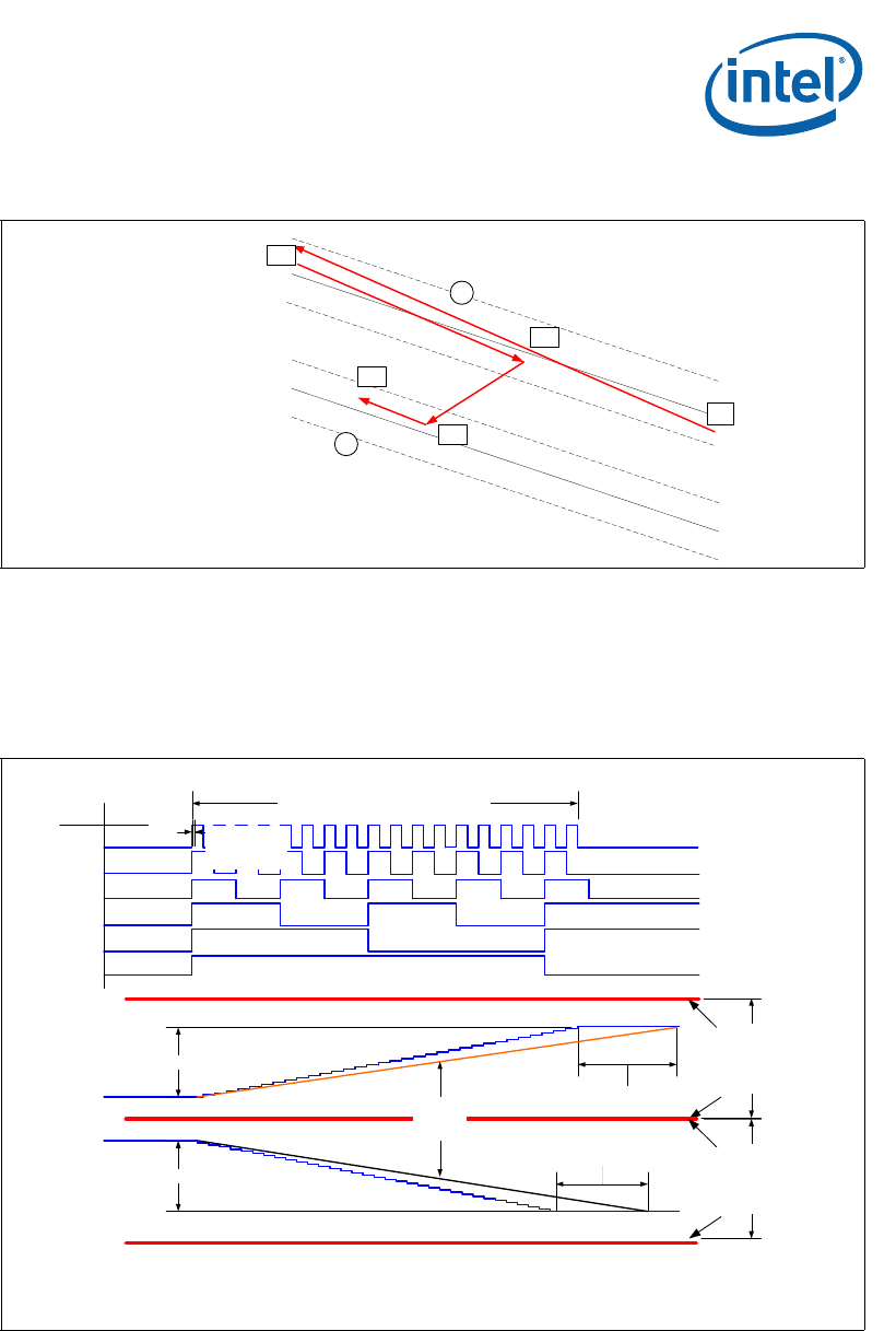
Figure 2-6. Dynamic VID Transition States Illustration
high VID to low VID
Vcc transition
450mV
50µs maximum settling
from registering final VID
450mV
low VID to high VID
Vcc transition
50µs maximum settling
from registering final VID
The diagram assumes steady state, constant current during the dynamic VID
transitions for ease of illustration; actual processor behavior allows for any dIcc/dt
event during the transitions, depending on the code it is executing at that time
VID 5
VID 0
VID 1
VID 2
VID 3
VID 4
36 VID steps @ 5 s each step = 180us
Upper equals
Final VID - 1.25 m * Icc
Lower equals
Start VID - 1.25 m * Icc - 30mV
Maximum
Vcc
settling
Upper equals
Final VID - 1.25 m * Icc
Lower equals
Start VID - 1.25 m * Icc - 30mV
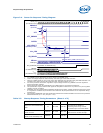
VID 1
VID 2
VID 3
VID 4
VID 5
VID 6
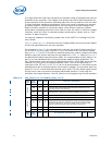
VR11
table
ext.
VR10
table
Note: VR11 table – VID 0 and extended VR10 table – VID 6 is reserved for future processors
400ns
worst case VID
settling time