MB91401
7
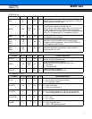
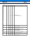
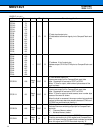
SYSTEM (9 pin)
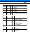
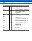
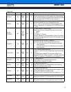
OSCILLATOR (3 pin)
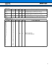
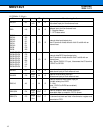
PLL CONTROL (5 pin)
Pin name Pin no.
Polarity
I/O
Circuit
Function/application
XINI 8 IN D
Clock input pin
Input pin of clock generated in clock generator. 10 MHz to
50 MHz frequency can be input.
INITXI 204
Nega-
tive
IN D
Reset input pin
This pin inputs a signal to initialize the LSI.
When turning on the power supply, apply “0” to the pin until
the clock signal input to the CLKIN pin becomes stable.
All built-in registers and external pins are initialized, and the
built-in PLL is stopped when “0” is asserted to INITXI.
NMIX 206
Nega-
tive
IN D
NMI input pin
Non-Maskable Interrupt signal
INT7
INT6
INT5
150
87
16
IN D
External interrupt input pins
These pins input an external interrupt request signal.
For external interrupt detection, set the ENIR, EIRR and
ELVR registers of the FR core.
MDI2
MDI1
MDI0
80
142
79
IN D
Mode pins
These pins determine the operation mode of the LSI.
Always set this bit to “001”.
Pin name Pin no.
Polarity
I/O
Circuit
Function/application
OSCEA 12 IN G
Crystal oscillation input pin
Input pin of crystal oscillation cell.
OSCC 145
Nega-
tive
IN D
Crystal oscillation control input pin
Oscillation control pin of crystal oscillation cell.
“0” : Oscillation
“1” : Oscillation stop
OSCEB 10 OUT G
Crystal oscillation output pin
Output pin of crystal oscillation cell.
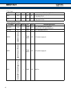
Pin name Pin no.
Polarity
I/O
Circuit
Function/application
PLLS 147 IN D
PLL/through mode (reset) switching input pin
“0” : PLL through mode (oscillation stop)
“1” : PLL oscillation mode
PLLSET1 144 IN D
Input clock division ratio select input pin
“0” : Input clock direct
“1” : Input clock divided by 2
PLLSET0 81 IN D
Division ratio select input to PLL FB pin
“0” : Two dividing frequency is input to the terminal FB.
“1” : Four dividing frequency is input to the terminal FB.
PLLBYPAS 9 IN D
PLL bypass select input pin
“0” : PLL used
“1” : PLL unused
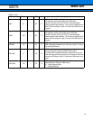
CLKSEL 77 IN D
Input clock switching input pin
“0” : XINI (External clock)
“1” : Built-in OSC generating clock
Prelminary
2004.11.12


