MB91401
20
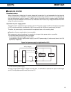
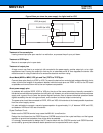
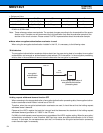
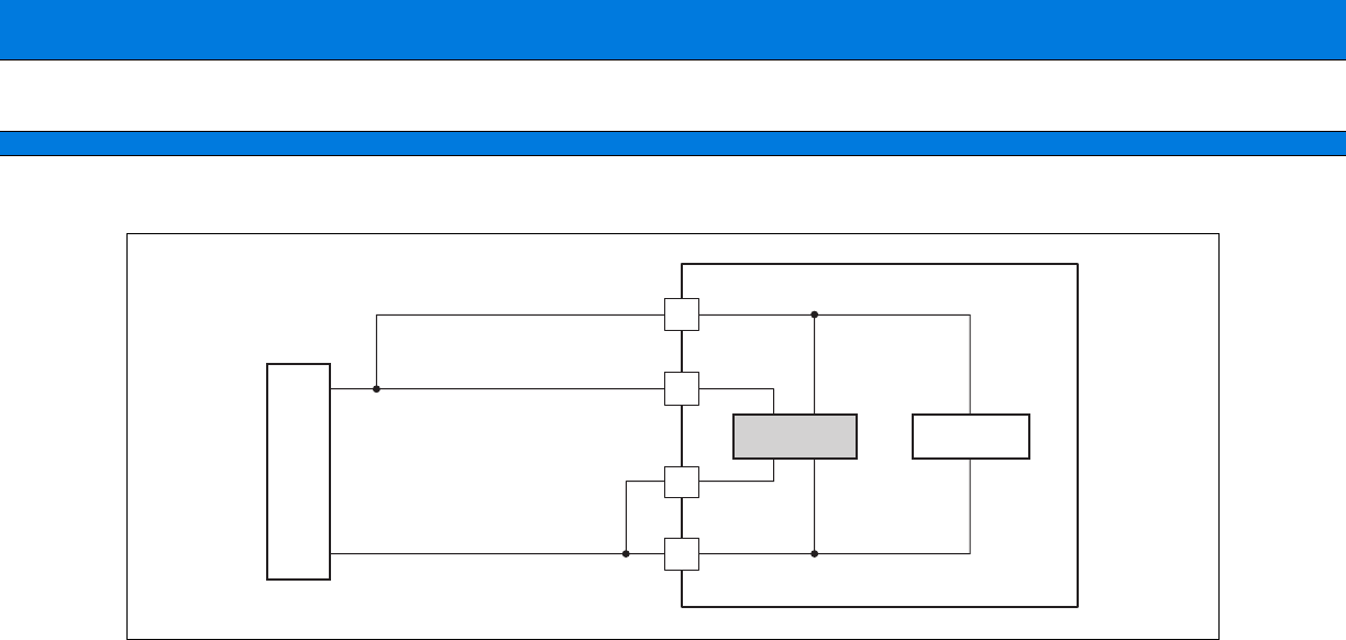
Figure When you share the power supply for digital and for VCO
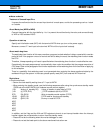
Treatment of the unused pins
Leaving unused input pins open results in a malfunction, so process the pull-up or pull-down.
Treatment of OPEN pins
Be sure to use open pins in open state.
Treatment of output pins
A large current may flow to an output pin left connected to the power-supply, another output pin, or to a high
capacitance load. Leaving the output pin that way for an extended period of time degrades the device. Use
meticulous care in using the device not to exceed the absolute maximum rating.
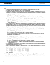
About Mode (MDI2 to MDI0, VPD) pin and Test (TEST3 to TEST0) pin
Connect these pins directly to VDDE or VSS. To prevent the device from entering test mode accidentally due to
noise, minimize the lengths of the patterns between individual mode pins and VDDE or VSS on the PC board
as possible and connect them with as low an impedance as possible.
About power supply pins
In products with multiple VDDE, VDDI or VSS pins, the pins of the same potential are internally connected in
the device to avoid abnormal operations including latch-up. However you must connect the pins to external power
supply and a ground line to lower the electro-magnetic emission level to prevent abnormal operation strobe
signals caused by the rise in the ground level, and to conform to the total output current rating.
The power pins should be connected to VDDE, VDDI and VSS of this device at the lowest possible impedance
from the current supply source.
It is also advisable to connect a ceramic bypass capacitor of approximately 0.1 µF between VDDE and VSS,
and between VDDI and VSS near this device.
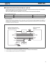
Crystal Oscillator Circuit
Noise near the OSCEA terminal may cause the MB91401 to malfunction.
Design the circuit board so that OSCEA terminal, OSCEB terminal and the crystal oscillator, and the bypass
capacitor to ground are located as close to the device as possible.
It is strongly recommended to design the PC board artwork with the OSCEA terminal and OSCEB terminal
surrounded by ground plane because stable operation can be expected with such a layout.
VSS
LSI
APLL
PLLVSS
VDD (for digital)
PLLVDD (for VCO)
Logic part
Power
supply
(a)
Prelminary
2004.11.12


