


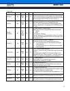
MB91401
19
■
■■
■
HANDLING DEVICES
Preventing Latch-up
When a voltage that is higher than V
DDE and a voltage that is lower than VSS are impressed to the input terminal
and the output terminal in CMOS IC or the voltage that exceeds ratings between V
DDE to VSS is impressed, the
latch-up phenomenon might be caused. If latch-up occurs, the supply current increases rapidly, sometimes
resulting in thermal breakdown of the device. Use meticulous care not to let any voltage exceed the maximum
rating during device operation.
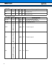
Separation of power supply pattern
Analog PLL (APLL at the following) is installed in this LSI. The power supply for VCO and for digital is separated
in LSI so that the oscillation characteristic of APLL may receive the influence of power supply variation.
Therefore, the power supply is recommended to be separated also on the mounting base.
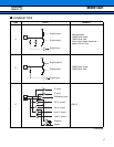
•
••
•
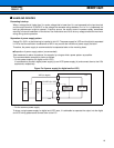
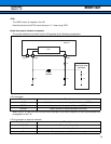
Separation of power supply pattern (recommended)
Take measures to reduce impedance, for example, by using as wide a power pattern as possible.
The recommendation example is shown as follows.
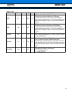
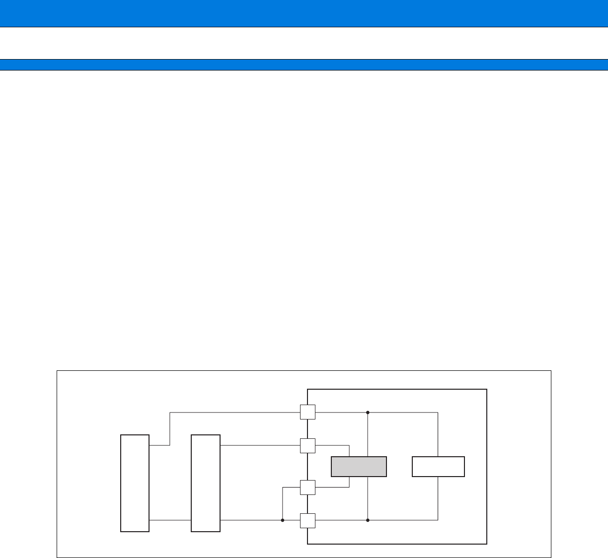
• For two power supplies (for digital and for VCO)
It is advisable to provide a digital power-supply (a) and VCO power-supply (b) and connect them to the LSI’s
equivalents, respectively.
Figure For 2-power supply (for digital and for VCO)
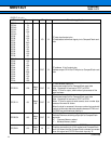
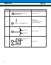
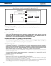
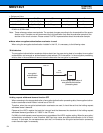
• For the common power supply
To share a single power-supply for digital and VCO uses, it is advisable to separate the output into the digital
and VCO wiring patternsand connect them to the LSI.
LSI
PLLVSS
APLL
VSS
VDD (for digital)
PLLVDD (for VCO)
Logic part
Power
supply
(a)
Power
supply
(b)
Prelminary
2004.11.12