


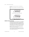
Chapter 4 VME-MXI-2 Configuration and Installation
VXI/VME-PCI8022 for Solaris 4-4
©
National Instruments Corporation
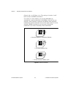
more information on setting base addresses on a multimainframe
hierarchy.
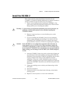
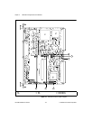
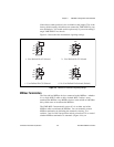
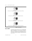
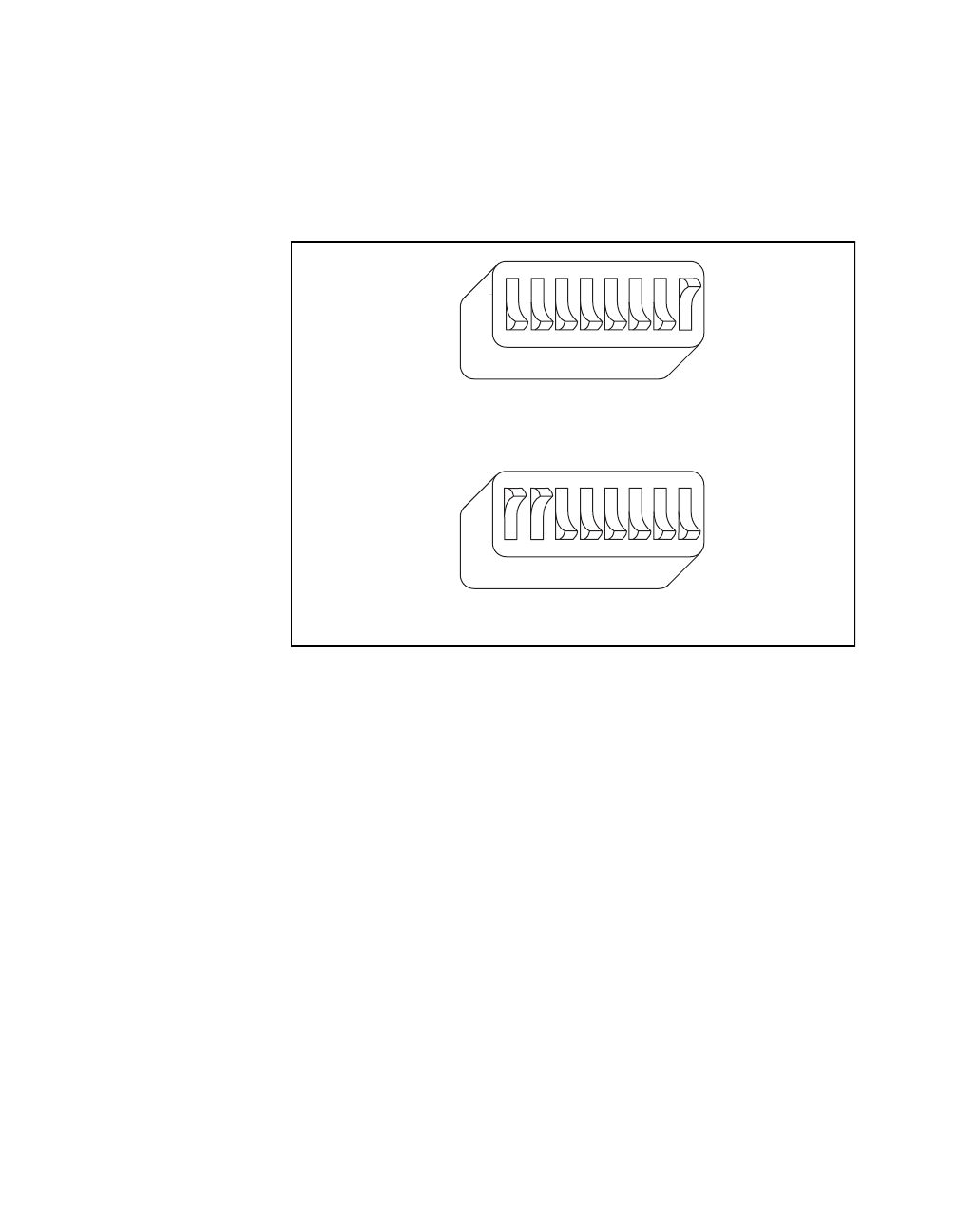
Figure 4-2 shows switch settings for A16 base address hex C040 and
F000.
Figure 4-2. Base Address Selection
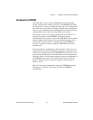
VME-MXI-2 Intermodule Signaling
If you will be installing more than one VME-MXI-2 in a single VMEbus
chassis, you must select a user-defined pin for use by the VME-MXI-2.
The VME-MXI-2 modules use this signal to disable the bus timeout
unit(s) on the other VME-MXI-2 modules during VMEbus accesses that
map to the MXIbus. This is done because the MXIbus bus timeout unit
should be the sole timer of any MXIbus access. Since bus timeout units
on other VMEbus modules cannot monitor this signal, they should be
permanently disabled. If it is not possible to disable a module’s bus
timeout unit, it should be configured to the highest setting to give
MXIbus accesses as much time as possible.
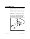
You can choose from three user-defined pins on J2/P2. The pin you
select must be bused on the VMEbus backplane between all slots that
will have a VME-MXI-2 installed. Use jumper W2 to select pin A5, C5,
or C30 of J2/P2, as shown in Figure 4-3.
a. Switch Set to A16 Base Address hex C040 (Default)
b. Switch Set to A16 Base Address Hex F000
OFF
1 2345678
U20
OFF
1 2345678
U20