


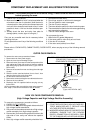
R-2397
20
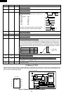
Pin No. Signal I/O Description
46 P10 OUT
Segment data signal.
Signal similar to P17.
47-48 P07-P06 OUT
Segment data signal.
Signal similar to P17.
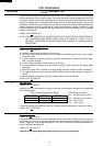
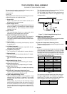
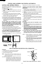
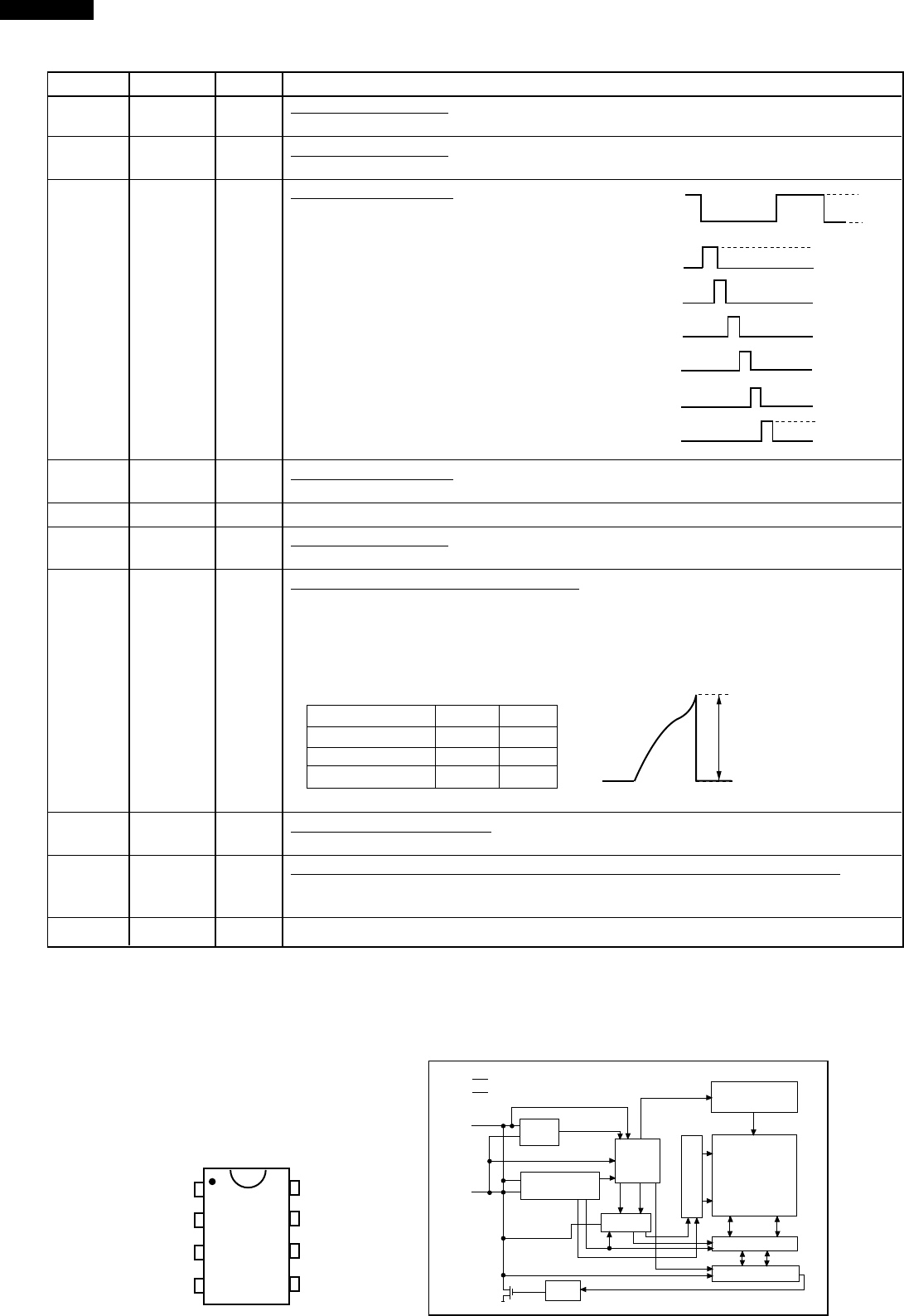
49 P05 OUT
Digit selection signal.
The relation between digit signal and digit are as
follows:
Digit signal Digit
P05 1st.
P04 2nd.
P03 3rd.
P02 4th.
P01 5th.
P00 6th.
Normally, one pulse is output in every ß period,
and input to the grid of the Fluorescent Display.
50-54 P04-P00 OUT Digit selection signal.
Signal similar to P16.
55-57 P27-P25 OUT Terminal not used.
58-59 P24-P23 OUT
Segment data signal.
Signal similar to P17.
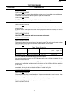
60 P22 OUT
(Sound) Voltage level control terminal.
This terminal (P22) is to control volume level of buzzer sound with terminals P21. Since
the volume level of buzzer sound depends on voltage energized, it is control level in 3
steps by combining signal levels for P22,P21. Relationship of signal level combination to
sound volume level is shown in the following table, 1~3 in the table, however, are indicated
in the descending order from the maximum level of sound volume through the minimum
level.
Sound Volume P21 P22
1,(Max.) L L
2, H L
3,(Min.) L H
*At Output terminal P32, rectangular wave signal of 2.5kHz is output.
61 P21 OUT
Sound level control signal.
Refer to above signal P22.
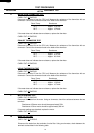
62 P20 IN
Input signal which communicates the door open/close information to LSI.
Door closed; "H" level signal(0V).
Door opened; "L" level signal(-31.0V).
63/64 AVCC/VCC IN Connected to GND.
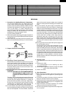
H
L
GND
ß(50Hz)
P05
P04
P03
P02
P01
P00
GND
-31(V)
-31(V)
A
A : 1,(Max) 20V
2, 13V
3,(Min) 7V
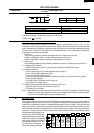
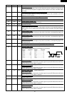
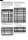
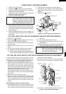
2-2 Memory IC (IC2)
AT24C04 is a 4K-bit, serial memory, enabling CMOS to be erased/written electrically. This memory is constructed with 512
registers x 8bits, enabling individual access, read and write operations to be performed. Details of input/output signal for IC2
are as shown in the following diagram.
1
A1
A2
VSS
VCC
TEST
SCL
SDA
TOP VIEW
A0
2
3
4
8
7
6
5
FUNCTIONAL DIAGRAM
E PROM
512 x 8
2
START
STOP
LOGIC
CONTROL
LOGIC
SLAVE ADDRESS
REGISTER
COMPARATOR
H.V. GENERATION
TIMING
& CONTROL
64
YDEC
8
DATA REGISTER
Dout
CK
3
1
5
64
XDEC
START CYCLE
INC
LOAD
WORD
ADDRESS
COUNTER
R/W
PIN
Dout
ACK
(6) SCL
(5) SDA
(4) Vss
(3) Vcc
Figure T-4 Relation between Pin Nos, and Signals