


Camera interfaces
Hardware Installation Guide V2.0.0
60
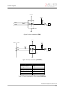
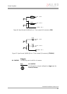
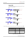
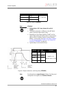
OutVCC Resistor value
5 V 1 kΩ
≈ 5 mA load12 V 2.4 kΩ
24 V 4.7 kΩ
Figure 40: OutVCC (STINGRAY)
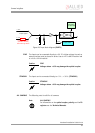
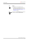
Note
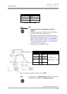
L
STINGRAY
• Voltage above +30 V may damage the optical
coupler.
• The output connection is different to the AVT Marlin
series to achieve higher output swing.
• Depending on the voltage applied at OutVCC and the
type of input which you want to drive, it may be neces-
sary to switch an external resistor in series between
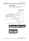
GPOut1...4 and ground. See Figure 38: Output schemat-
ics with external resistors R (pin no. from camera I/O
connector) (STINGRAY) on page 59.
• Typical delay is not more than 40 µs.
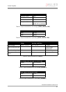
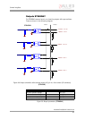
Figure 41: Output schematics: switching times (STINGRAY)
Note
L
For information on output features (IntEna, Fval, Busy) and
configuration via registers see Technical Manuals.
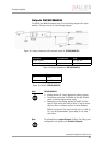
Parameter Sym-
bol
Value
(TLP281)
Condition
Delay time t
d
0.78 µs
OutVCC = 5 V
Resistor value = 1 kΩ
Rise time t
r
0.65 µs
Storage
time
t
s
27.6 µs
Fall time t
f
11 µs