EM78P221/2N
8-Bit Microcontroller with OTP ROM
16 •
Product Specification (V1.0) 10.19.2007
(This specification is subject to change without further notice)
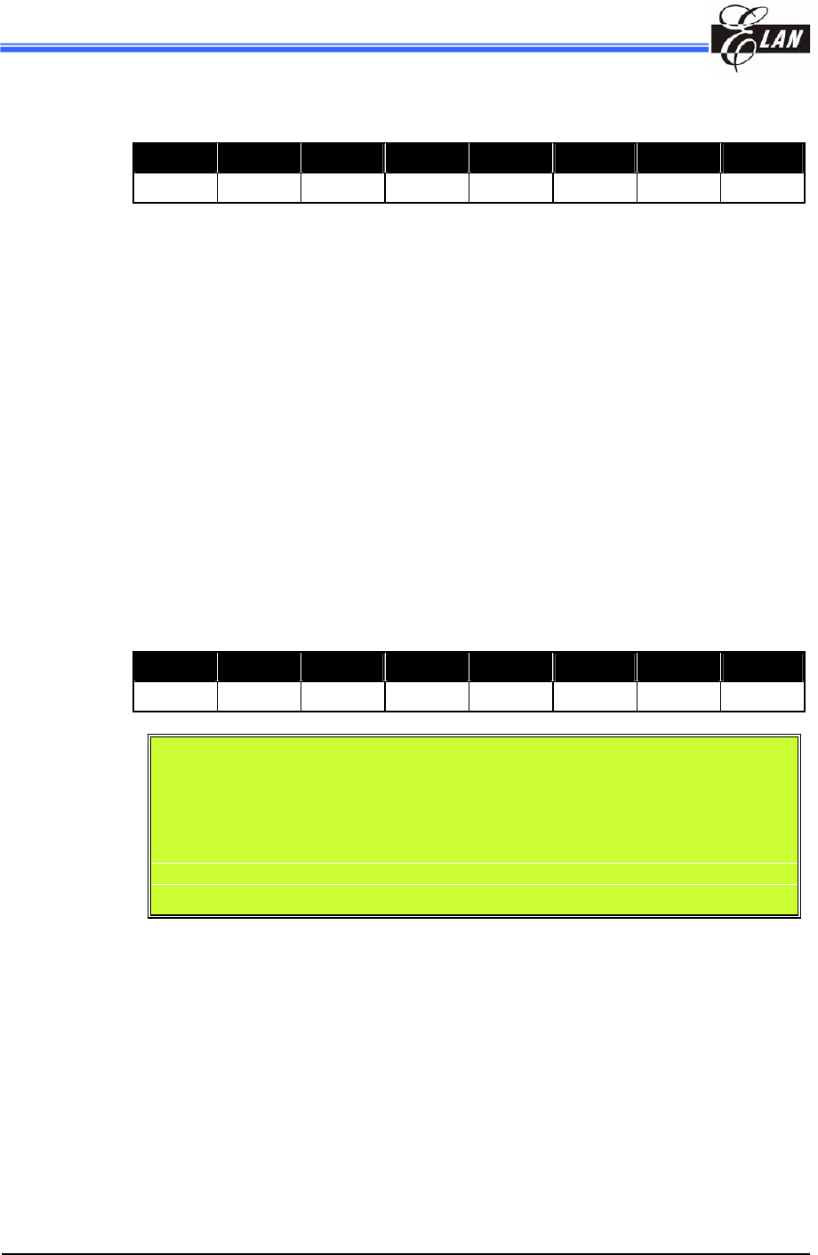
6.2.21 Bank 1-RD (Pull-high Control Register)
Bit 7 Bit 6 Bit 5 Bit 4 Bit 3 Bit 2 Bit 1 Bit 0
/PH7 /PH6 /PH5 /PH4 /PH3 /PH2 /PH1 /PH0
Bank 1-RD register is both readable and writable.
Bit 7 (/PH7): Control bit used to enable the pull-high function of the P67 pin.
0 = Enable internal pull-high
1 = Disable internal pull-high
Bit 6 (/PH6): Control bit used to enable the pull-high function of the P66 pin.
Bit 5 (/PH5): Control bit used to enable the pull-high function of the P65 pin.
Bit 4 (/PH4): Control bit used to enable the pull-high function of the P64 pin.
Bit 3 (/PH3): Control bit used to enable the pull-high function of the P53 pin.
Bit 2 (/PH2): Control bit used to enable the pull-high function of the P52 pin.
Bit 1 (/PH1): Control bit used to enable the pull-high function of the P51 pin.
Bit 0 (/PH0): Control bit used to enable the pull-high function of the P50 pin.
6.2.22 Bank 1-RE (WDT Control Register)
Bit 7 Bit 6 Bit 5 Bit 4 Bit 3 Bit 2 Bit 1 Bit 0
WDTE 0 PSWE PSW2 PSW1 PSW0 0 CMPIE
NOTE
Bank 1-RE <0> register is both readable and writable
Individual interrupt is enabled by setting its associated control bit in the
Bank 1-RF <0 > to "1."
Global interrupt is enabled by the ENI instruction and is disabled by the DISI
instruction. Refer to Fig. 6-8 (Interrupt Input Circuit) under Section 6.6
(Interrupt).
Bit 7 (WDTE): Control bit is used to enable Watchdog Timer
0 = Disable WDT
1 = Enable WDT
WDTE is both readable and writable.
Bits 6, 1: not used, fixed to 0 all the time
Bit 5 (PSWE): Prescaler enable bit for WDT
0 = prescaler disable bit. WDT rate is 1:1
1 = prescaler enable bit. WDT rate is set as Bit 4~Bit 2


