


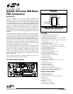
Si4421
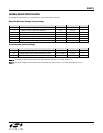
GENERAL DEVICE SPECIFICATIONS
All voltages are referenced to V
ss
, the potential on the ground reference pin VSS.
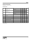
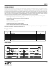
Absolute Maximum Ratings (non-operating)
Symbol Parameter Min Max Units
V
dd
Positive supply voltage -0.5 6 V
V
in
Voltage on any pin (except RF1 and RF2) -0.5 V
dd
+0.5 V
V
oc
Voltage on open collector outputs (RF1, RF2) -0.5 V
dd
+1.5 (Note 1) V
I
in
Input current into any pin except VDD and VSS -25 25 mA
ESD Electrostatic discharge with human body model 1000 V
T
st
Storage temperature -55 125
o
C
T
ld
Lead temperature (soldering, max 10 s) 260
o
C
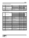
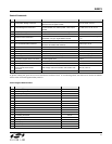
Recommended Operating Range
Symbol Parameter Min Max Units
V
dd
Positive supply voltage 2.2 3.8 V
V
oc
Voltage range on open collector outputs (RF1, RF2) V
dd
-1.5 (Note 2) V
dd
+1.5 V
T
op
Ambient operating temperature -40 85
o
C
Note 1: The voltage on RF1 and RF2 pins can be higher than the actual V
dd
but cannot exceed 7 V.
Note 2: The actual voltage on RF1 and RF2 pins can be lower than the current V
dd
but never should go below 1.2 V.
8