


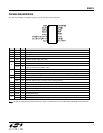

Si4421
Note 1: Measured with disabled clock output buffer
Note 2: Not using a 10 MHz crystal is allowed but not recommended because all crystal referred timing and frequency parameters
will change accordingly
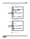
Note 3: See the BER diagrams in the measurement results section (page 37) for detailed information
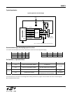
Note 4: See reference design with 50
Ohm Matching Network (page 39) for details
Note 5: See reference design with Resonant PCB Antenna (BIFA) on page 41 for details
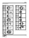
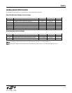
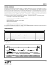
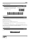
Note 6: Optimal antenna admittance/impedance:
Si4421 Y
antenna
[mS] Z
antenna
[Ohm] L
antenna
[nH]
433 MHz 2 – j5.9 52 + j152 62
868 MHz 1.2 - j11.9 7.8 + j83 15.4
915 MHz 1.49 - j12.8 9 + j77 13.6
Note 7: Adjustable in 8 steps
Note 8: During the Power-On Reset period, commands are not accepted by the
chip. In case of software reset (see Wake-Up Timer
Command, page 25) the reset timeout is 0.25ms typical.
Note 9: The crystal oscillator start up time strongly depends on the cap
acitance seen by the oscillator. Low capacitance and low
ESR crystal is recommended with low parasitic PCB layout design.
Note 10: By design
12