


Si4421
CONTROL INTERFACE
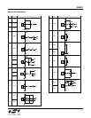
Commands to the transmitter are sent serially. Data bits on pin SDI are shifted into the device upon the rising edge of the clock on
pin SCK whenever the chip select pin nSEL is low. When the nSEL signal is high, it initializes the serial interface. All commands
consist of a command code, followed by a varying number of parameter or data bits. All data are sent MSB first (e.g. bit 15 for a 16-
bit command). Bits having no influence (don’t care) are indicated with X. Special care must be taken when the microcontroller’s built-
in hardware serial port is used. If the port cannot be switched to 16-bit mode then a separate I/O line should be used to control the
nSEL pin to ensure the low level during the whole duration of the command or a software serial control interface should be
implemented. The Power-On Reset (POR) circuit sets default values in all control and command registers.
The receiver will generate an interrupt request (IT) for the microcontroller - by pulling the nIRQ pin low - on the following events:
The TX register is ready to receive the next byte (RGIT)
The RX FIFO has received the preprogrammed amount of bits (FFIT)
Power-on reset (POR)
RX FIFO overflow (FFOV) / TX register underrun (RGUR)
Wake-up timer timeout (WKUP)
Negative pulse on the interrupt input pin nINT (EXT)
Supply voltage below the preprogrammed value is detected (LBD)
FFIT and FFOV are applicable when the RX FIFO is enabled. RGIT and RGUR are applicable only when the TX register is enabled. To
identify the source of the IT, the status bits should be read out.
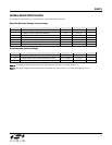
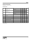
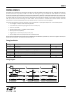
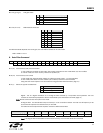
Timing Specification
Symbol Parameter Minimum value [ns]
t
CH
Clock high time 25
t
CL
Clock low time 25
t
SS
Select setup time (nSEL falling edge to SCK rising edge) 10
t
SH
Select hold time (SCK falling edge to nSEL rising edge) 10
t
SHI
Select high time 25
t
DS
Data setup time (SDI transition to SCK rising edge) 5
t
DH
Data hold time (SCK rising edge to SDI transition) 5
t
OD
Data delay time 10
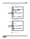
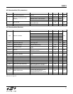
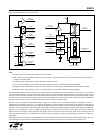
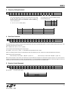
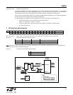
Timing Diagram
SCK
SDI
SDO
nSEL
t
DS
t
DH
t
CH
t
CL
BIT15 BIT14 BIT13
t
SS
BIT8 BIT7
t
OD
OFFS (0) FIFO OUT
BIT1 BIT0
t
SH
t
SHI
FFIT FFOV ATSCRL
13