


Si4421
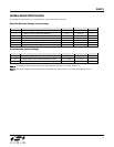
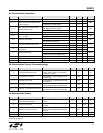
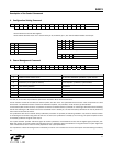
AC Characteristics (Transmitter)
Symbol Parameter Conditions/Notes Min Typ Max Units
I
OUT
Open collector output DC current Programmable 0.5 6 mA
In 433 MHz band 7
P
max_50
Max. output power delivered to 50
Ohm load over a suitable matching
network (Note 4)
In 868 MHz / 915 MHz bands 5
dBm
In 433 MHz band with monopole antenna
with matching network (Note 4)
7
P
max_ant
Max. EIRP with suitable selected
PCB antenna (Note 6)
In 868 MHz / 915 MHz bands (Note 5) 7
dBm
P
out
Typical output power Selectable in 2.5 dB steps (Note 7) P
max
-17.5 P
max
dBm
At max power 50 Ohm load (Note 4) -55
P
sp
Spurious emission
l f-f
sp
l
> 1 MHz
With PCB antenna (Note 5) -60
dBc
At max power 50 Ohm load (Note 4) -35
P
harm
Harmonic suppression
With PCB antenna (Note 5) -42
dBc
In 433 MHz band 2 2.6 3.2
C
o
Output capacitance (set by the
automatic antenna tuning circuit)
In 868 MHz / 915 MHz bands 2.1 2.7 3.3
pF
In 433 MHz band 13 15 17
Q
o
Quality factor of the output
capacitance
In 868 MHz / 915 MHz bands 8 10 12
100 kHz from carrier, in 868 MHz band -80
L
out
Output phase noise
1 MHz from carrier, in 868 MHz band -103
dBc/Hz
BR
TX
FSK bit rate Via internal TX data register 172 kbps
BRA
TX
FSK bit rate TX data connected to the FSK input 256 kbps
df
fsk
FSK frequency deviation Programmable in 15 kHz steps 15 240 kHz
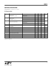
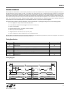
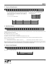
AC Characteristics (Turn-on/Turnaround timings)
Symbol Parameter Conditions/Notes Min Typ Max Units
t
sx
Crystal oscillator startup time
Default capacitance bank setting, crystal
ESR < 50 Ohm (Note 9). Crystal load
capacitance = 16 pF.
2 7 ms
T
tx_XTAL_ON
Transmitter turn-on time
Synthesizer off, crystal oscillator on with
10 MHz step
250 µs
T
rx_XTAL_ON
Receiver turn-on time
Synthesizer off, crystal oscillator on with
10 MHz step
250 µs
T
tx_rx_SYNT_ON
Transmitter – Receiver turnover time
Synthesizer and crystal oscillator on
during TX/RX change with 10 MHz step
150 µs
T
rx_tx_SYNT_ON
Receiver – Transmitter turnover time
Synthesizer and crystal oscillator on
during RX/TX change with 10 MHz step
150 µs
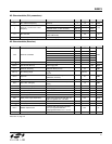
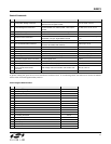
AC Characteristics (Others)
Symbol Parameter Conditions/Notes Min Typ Max Units
C
xl
Crystal load capacitance,
see crystal selection guide
Programmable in 0.5 pF steps, tolerance
± 10%
8.5 16 pF
t
POR
Internal POR timeout
After V
dd
has reached 90% of final value
(Note 8)
100 ms
t
PBt
Wake-up timer clock accuracy
Crystal oscillator must be enabled to
ensure proper calibration at the start up.
(Note 9)
± 10 %
C
inD
Digital input capacitance 2 pF
t
r
, t
f
Digital output rise/fall time 15 pF pure capacitive load 10 ns
Notes are on page 12.
11