


Si4421
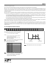
RX FIFO BUFFERED DATA READ
In this operating mode, incoming data are clocked into a 16-bit FIFO buffer. The receiver starts to fill up the FIFO when the Valid Data
Indicator (VDI) bit and the synchron pattern recognition circuit indicates potentially real incoming data. This prevents the FIFO from
being filled with noise and overloading the external microcontroller.
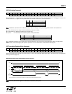
Interrupt Controlled Mode:
The user can define the FIFO IT level (the number of received bits) which will generate the nFFIT when exceeded. The status bits
report the changed FIFO status in this case.
Polling Mode:
When nFFS signal is low the FIFO output is connected directly to the SDO pin and its content can be clocked out by the SCK. Set the
FIFO IT level to 1. In this case, as long as FFIT indicates received bits in the FIFO, the controller may continue to take the bits away.
When FFIT goes low, no more bits need to be taken.
An SPI read command is also available to read out the content of the FIFO (Receiver FIFO Read Command, page 21).
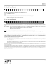
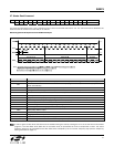
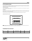
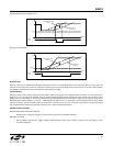
FIFO Read Example wit
h FFIT Polling
nSEL
SCK
nFFS
SDO
0
1234
FO+1 FO+2FIFO OUT FO+4FO+3
FIFO read out
FFIT
Note: During FIFO access f
SCK
cannot be higher than f
ref
/4, where f
ref
is the crystal oscillator frequency. When the duty-cycle of the
clock signal is not 50% the shorter period of the clock pulse should be at least 2/f
ref
.
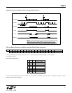
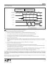
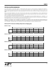
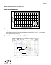
RECOMMENDED PACKET STRUCTURES
Preamble
Synchron word
(Can be network ID)
Payload CRC
Minimum length 4 - 8 bits (1010b or 0101b) D4h (programmable) ? 4 bit - 1 byte
Recommended length 8 -12 bits (e.g. AAh or 55h) 2DD4h (D4 is programmable) ? 2 byte
31