


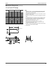
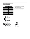
RC4194 PRODUCT SPECIFICATION
7
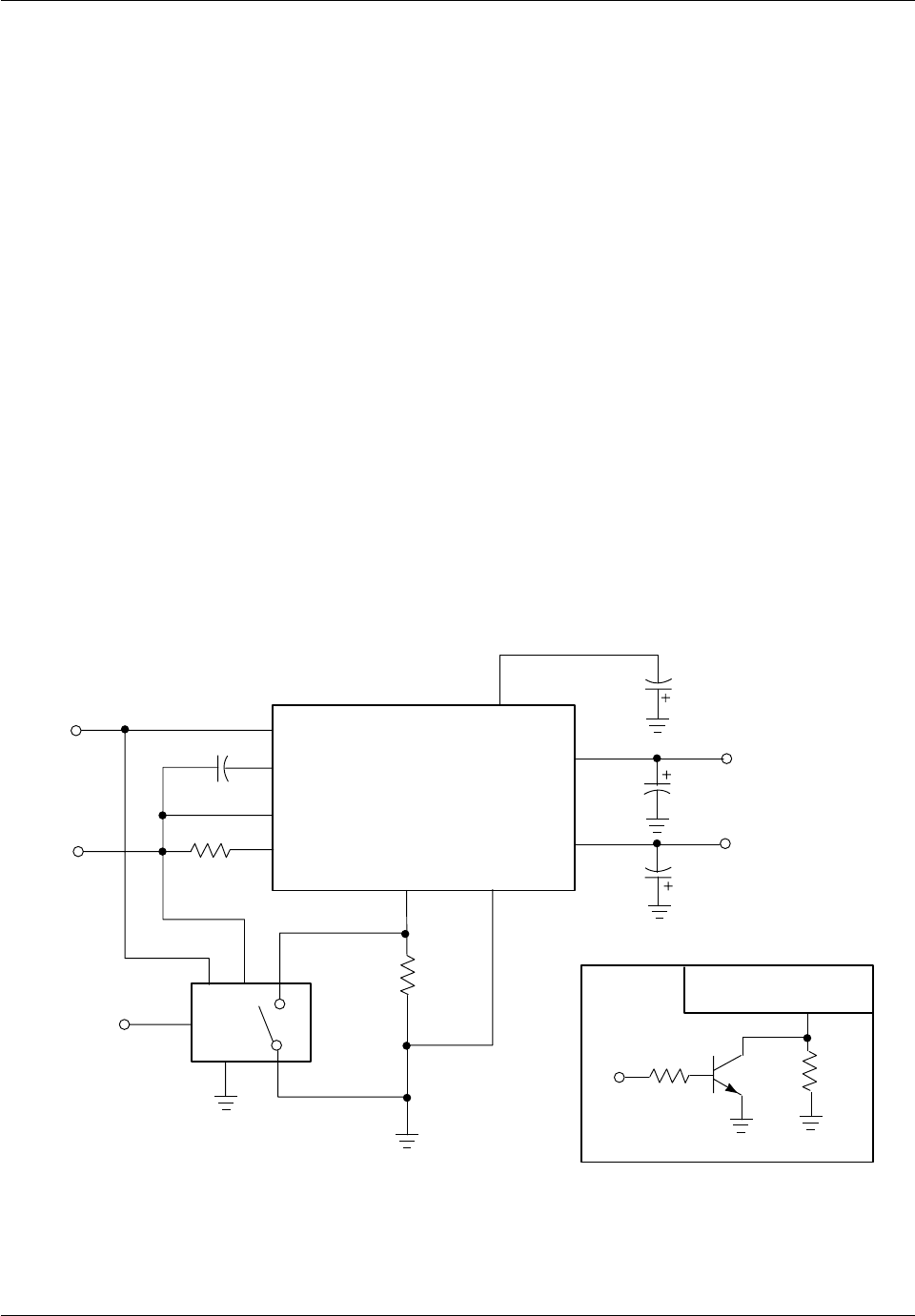
RC4194 Switchable Power Supply
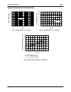
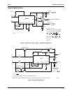
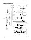
The outputs of the RC4194 can be simultaneously switched
on or off under logic control as shown in Figure 8. In the
“off” state, the outputs will be forced to a minimum voltage,
or about ±20 mV, rather than becoming open-circuit. The
turn-on time, with the outputs programmed to ±12V, is
approximately 200 mS. This circuit works by forcing the R0
pin to ground with an analog switch.
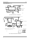
Refer to the RC4194 internal schematic diagram. A refer-
ence voltage that regulates with respect to –V
S
is generated
at the RSET pin by the zener diode Q12 and the buffer cir-
cuit of Q11 and Q13. When the external 71.5k RSET resis-
tor is connected between the R
SET
pin and –V
S
, a precision
current of 100 mA is generated which then flows into Q13’s
collector. Since Q13’s collector is tied to the R0 pin, the 100
mA current will develop a ground-referenced voltage drop
proportional to the value of R0, which is then amplified by
the internal error amplifier. When the analog switch in Fig-
ure 8 turns on, it effectively shorts out R0 and causes 0V to
be applied to the error amplifier. The output voltage in the
off state will be approxi-mately ±20 mV. If a higher value
(50 to 100 mV) is acceptable, then the DG201 analog switch
can be replaced with a low-cost small signal transistor, as
shown in the alternate switch configuration.
Compensation
For most applications, the following compensation technique
is sufficient. The positive regulator section of the RC4194 is
compensated by a 0.001 mF ceramic disc capacitor from the
Comp+ terminal to ground. The negative regulator requires
compensation at two points. The first is the Comp– pin,
which should have 0.001 mF to the –V
S
pin, or case. A
ceramic disc is ideal here. The second compen-sation point
for the negative side is the –V
OUT
terminal, which ideally
should be a 4.7 mF solid tantalum capacitor with enough
reserve voltage capacity to avoid the momentary shorting
and reforming which can occur with tantalum caps. For sys-
tems where the cost of a solid tantalum capacitor cannot be
justified, it is usually sufficient to use an aluminum capacitor
with a 0.03 mF ceramic disc in parallel to bypass high fre-
quencies. In addition, if the rectifier filter capacitors have
poor high frequency characteristics (like aluminum electro-
lytics) or if any impedance is in series with the +V
S
and –V
S
terminals, it is necessary to bypass these two points with
0.01 mF ceramic disc capacitors. Just as with monolithic op
amps, some applications may not require these bypass caps,
but if in doubt, be sure to include them.
Figure 8. ±12V Switchable Power Supply
65-4083
Comp+
+V
OUT
–V
OUT
4.7 µF
C
0.001 µF
4.7 µF
+12V
-12V
R
30K
4194
R
Gnd
+V
S
Comp–
–V
S
R
SET
R
SET
71.5K
0.001 F
m
+V
-V
Logic
–V
S
+V
S
Gnd
DG201
S
S
0
0
* Alternate Switch Configuration
4194
R
0
47K
30K
2N3904
*
*Quad SPST CMOS Analog Switch