


Physical Pinout Description
2-3
Analog Interface
2.4 Physical Pinout Description
Samtec part numbers SSW-110-22-F-D-VS-K and TSM-110-01-T-DV-P
provide a convenient 10-pin dual row header/socket combination at P1. This
header/socket provides access to the analog input pins of the TLV2553/6.
Consult Samtec at www.samtec.com
or 1−800−SAMTEC−9 for a variety of
mating connector options.
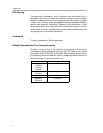
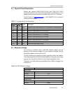
Table 2−1.Analog Input Pinout Description
Pin Number
Header Socket
Signal Description
P1.2 J1.2 CH0 Channel 0 input, can be direct from P1/J1 connector or through Op-Amp
P1.4 J1.4 CH1 Channel 1 input, direct from P1/J1 connector
P1.6 J1.6 CH2 Channel 2 input, direct from P1/J1 connector
P1.8 J1.8 CH3 Channel 3 input, direct from P1/J1 connector
P1.10 J1.10 CH4 Channel 4 input, direct from P1/J1 connector
P1.12 J1.12 CH5 Channel 5 input, direct from P1/J1 connector
P1.14 J1.14 CH6 Channel 6 input, direct from P1/J1 connector
P1.16 J1.16 CH7 Channel 7 input, direct from P1/J1 connector
P1.18 J1.18 REF− External Reference negative input
P1.20 J1.20 REF+ External Reference positive input
2.5 Reference Voltage
The accuracy of conversion from a SAR ADC depends directly upon the
accuracy of the reference voltage. It is very important, therefore, that the
reference be stable, accurate and low drift.
The ADC reference pin presents a dynamic capacitive load to the amplifier.
The voltage supplied to the ADC must be capable of driving this dynamic load
properly, ensuring that the reference remain stable regardless of load.
The bipolar and unipolar devices are specified to use a different voltage for the
reference pin.
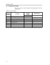
Table 2−2.ADC Reference Voltage
ADC Reference Voltage
Bipolar input
TLC3578 3.3 V
TLC3574 3.3 V
TLC2578 3.3 V
TLC2574 3.3 V
Unipolar input
TLC3548 4.096 V
TLC3544 4.096 V