Analog Interface Block Diagram
2-2
2.1 Analog Interface Block Diagram
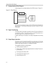
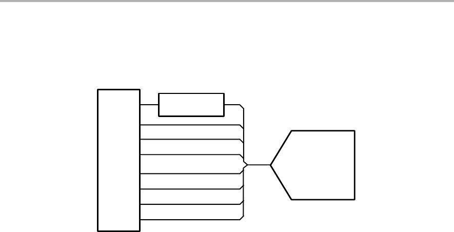
A block diagram for the analog interface of the EVM is shown in Figure 2−1.
Figure 2−1. Block Diagram
TLC3578
TLC3574
TLC3548
TLC3544
TLC2578
TLC2574
Signal
Conditioning
P1 / J1
The channels are arranged to comply with the EVM standard developed for
data converters. This standard defines eight channels of analog I/O on each
EVM module.
2.2 Signal Conditioning
The facility exists for the signal connected to channel 0 to be conditioned via
an operational amplifier. The amplifier present on the EVM operates from a
dual power supply and is configured with a gain of +1.
If signal conditioning is not required, it can easily be bypassed via a shorting
bar.
2.3 Single Supply Operation
Should the user wish to operate the amplifier from a single suply rail, this is also
possible by simply removing the dual supply amplifier and replacing it with a
suitable single supply alternative, for example the OPA353.
The suggested procedure is detailed below:
- Carefully desolder amplifier, U1
- Replace with a suitable single-supply alternative, for example TI part num-
ber OPA353UA
- Install appropriate resistor at R9
- Install appropriate capacitor at C11
- Install shorting bar at W1


