6 C1005M-G (10/02)
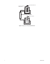
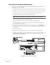
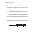
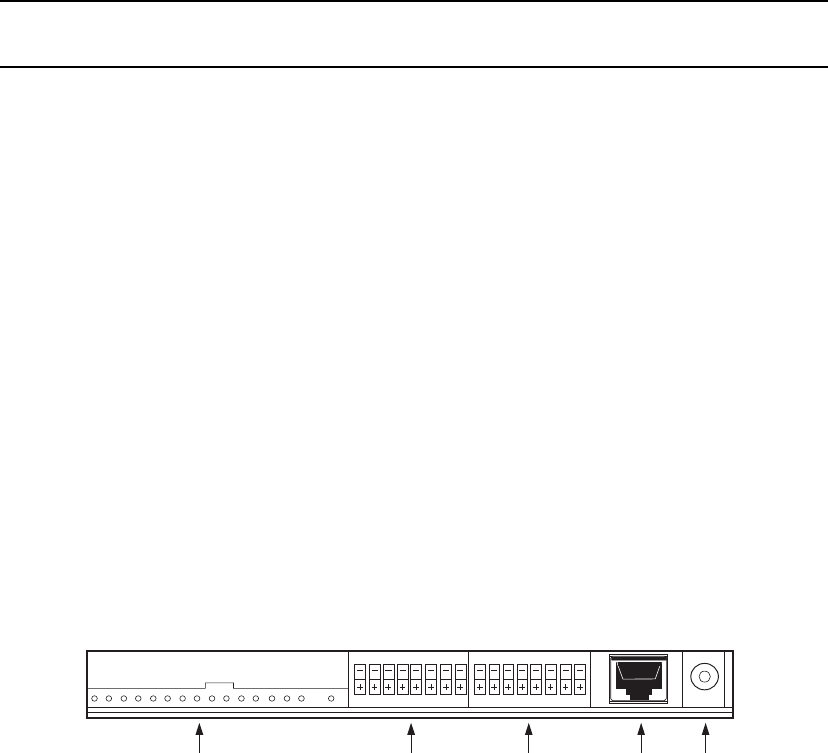
Figure 4. ICI1000PIM Switch Locations
12345678
ON
12345678
REGISTER/INTERFACE I PUTN BANK 1 BANK 2 DATA POWER
ON
CONFIGURING DIP SWITCH BANK 1
The switches in this bank serve several purposes. Selections include polling or non-polling operation, PIM addressing, clock
signal manipulation, and ICI1000PIM graphics mode selection.
The following describes the DIP switch settings for bank 1 on the ICI1000PIM. (Refer to Figure 4 and Tables A and B).
NOTE: If data is garbled or non-existent and you have set the DIP switches correctly for your register, try setting switch 1 on
bank 1 to the opposite position of the standard setting that Pelco indicated.
Switch 1 This switch selects either the inverted or non-inverted clock signal. The switch setting varies depending on the
register/interface type selected for switch bank 2 from Table B.
Switch 2 This switch selects either polling or non-polling operation. Non-polling mode should be selected when using
the ICI1000SE or ICI1000SI Inter-Check. This mode is defined with a plus [+] switch setting.
The DX2000 already is set for non-polling, even in PIM graphics mode.
Switch 3 The function of this switch depends on the register/interface type used. In dot matrix cash register
applications, this switch selects either normal [–] or PIM graphics [+] mode. Other applications have selections
for monitor display of receipt or journal information. This switch is normally in the closed [–] position.
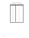
Switches 4-8 These switches set the addresses of multiple PIMs in a party-line system. The address selected normally will
coincide with the actual cash register number. The switch settings that correspond to PIM addresses are listed
in Table A.
CONFIGURING DIP SWITCH BANK 2
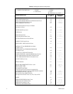
The switches in DIP switch bank 2 select the type of register/interface the ICI1000PIM interfaces. Table B indicates the switch
settings for specific register/interfaces. The first three switch settings have the same functions as switches 1-3 on DIP switch
bank 1. Refer to the
Configuring DIP Switch Bank 1
section for detailed descriptions of these three switches.
Refer to Figure 4 and Table B to set the switches in bank 2.


