


– 18 –
!
Qualified Service Personnel Only
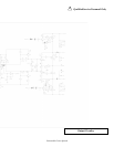
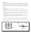
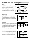
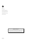
Class-G Trans•ana Amplifier
The transistor Q8 is configured as a
switch, which controls the current
source Q5, of the input differential
amplifier Q11 and Q12. If the power
On/Off, Signal Sensing, and Thermal
Protection circuits have all stopped
pulling to -15V, the turn-on process
begins, and the voltage at the emitter
of O8 slowly ramps up to zero Volts
according to the charging time of soft
start components R13, C93, and C94.
15V is divided between R40 and R65,
and imposed across the base-emitter
of Q5 and R35, causing current
source Q5 to turn the amplifier on.
The input signal is connected across
the differential amp transistors Q11
and Q12. U2B is configured as a DC-
servo integrater to null any DC at the
output.
The output of the differential amplifier
is fed to the positive pre-driver Q18,
and to the curent mirror which mirrors the inverted input current of Q6 into O7 and delivers it to the negative pre-driver
Q17. The pre-driver current is split between the three current paths of the bias and the driver circuit according to the factory
bias setting of trimpot R9, and the temperature of Q37. Q37 is thermally linked to the heatsink, and compensates for the
gate-voltage temperature coefficient of the output MOSFETs. Q19 drives the positive output MOSFET Q4, and Q21 drives the
negative output MOSFET Q10. Local feedback components C47 and R86 help to stabilize this output stage.
At low output voltages, current flows to the woofer from the lower voltage rail +LV or -LV through the diodes CR1/CR17 and
output MOSFETs Q4/Q10. When the output voltage approaches or exceeds these lower voltage rails, output current flows
from the higher voltage rail +HV or -HV through CLASS-G MOSFET Q9/Q1 and output MOSFETS Q4/Q10.
Positive G driver Q13 turns on class G MOSFET Q9 when the base-emitter voltage exceeds 0.7V. This occurs when
(OUT - 1.4 - 5.1V) - (+LV - 0.7 - 10) > 0.7V, which reduces to OUT > +LV - 3.5V. A similar equation can be applied to the
negative class G driver Q23. The resulting behavior can be observed as the class G rail on the source of the output MOSFET
tracking 3.5V higher (or lower) than the output signal.
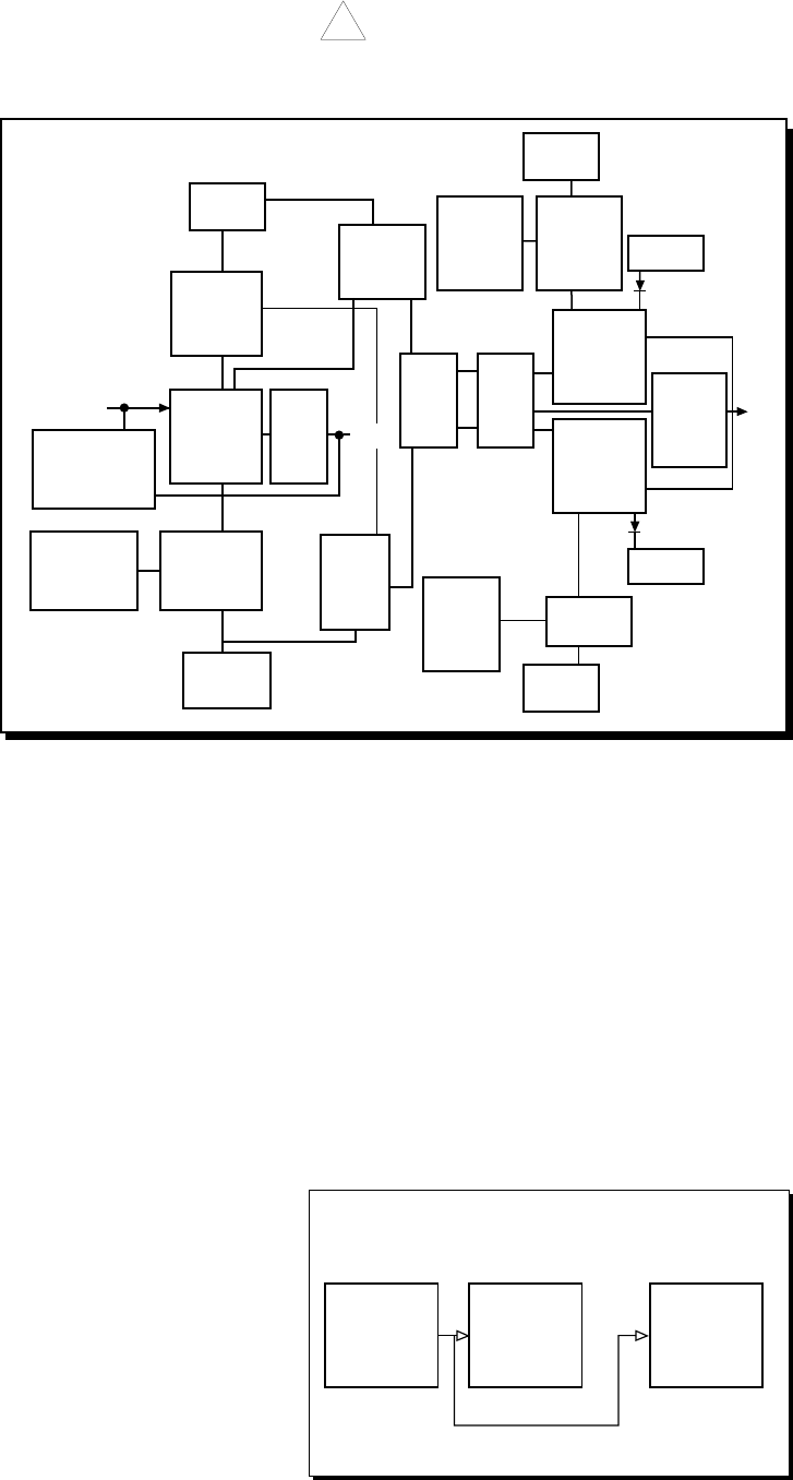
Soft Start Circuit
The amplifier soft start circuit is controlled by three On/Off circuits:
Power On/Off, Signal Sensing, and Thermal Protection. The "diode
OR" connection of CR5, CR6, and CR3 causes the amplifier to turn off
if power On/Off is low or Signal Sensing is low or the Thermal Protec-
tion is low. The amplifier will turn on only if all these circuit outputs
are high. In this all-high condition, CR5, CR6, and CR3 are open
circuited or back-biased, allowing R13 to turn on Q2 and Q8, illumi-
nating LED CR8 and turning on the amplifier. Q8 is turned on slowly,
according to the time constant of R13 and C93 and C94. This "soft
start" behavior eliminates audible turn on transients.
SOFT START CIRCUIT
ON / OFF
CR5
CR6
CR3
ON
INDICATOR
LED
Q2
R50
CR8
R13
C93
C94
Q8
SOFT
START
DELAY
R13
C93
C94
Q8
SOFT
START
DC
OFFSET
U2B, R47, C22
DIFF
AMP
Q11, Q12
I MIRROR
Q6, Q7
+ 15V
AMPLIFIER
+HV
-HV
FB
R46
C10
I
SOURCE
R40, R65
Q5,R35
NEG PRE-
DRIVER
Q17
POS PRE-
DRIVER
Q18
BIAS
Q37
R9
OUT
DRIVER
Q19
Q21
POS
OUT
Q4
LOCAL
FB
C47
R86
NEG
OUT
Q10
-LV
POS
G
DRIVER
Q13
NEG
G
DRIVER
Q23
POS
G
Q9
+LV
CR1
- 15V
NEG
G
Q1
<out
CR17
out